Simple Pipelined Processor Overview
I took a computer architecture class as part of my graduate degree. The final project for the class involved a pencil and paper project where we had to design a simple pipelined processor and describe its architecture. The processor has five stages: fetch, decode, execute, memory and write back. I decided to go all out and implement my processor in FPGA software. We were assigned two simple programs out of a total of five that we had to write to perform some simple task such as array value accumulation. I figured since I put in the time to design and simulate the processor, I would complete all five programming tasks. Below is the link to the original project guidelines:
Pipelined Processor Project SpecificationThe following link is the final report I turned in based on the processor I designed:
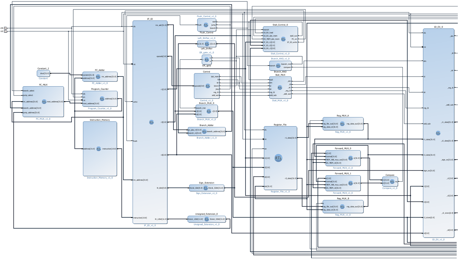
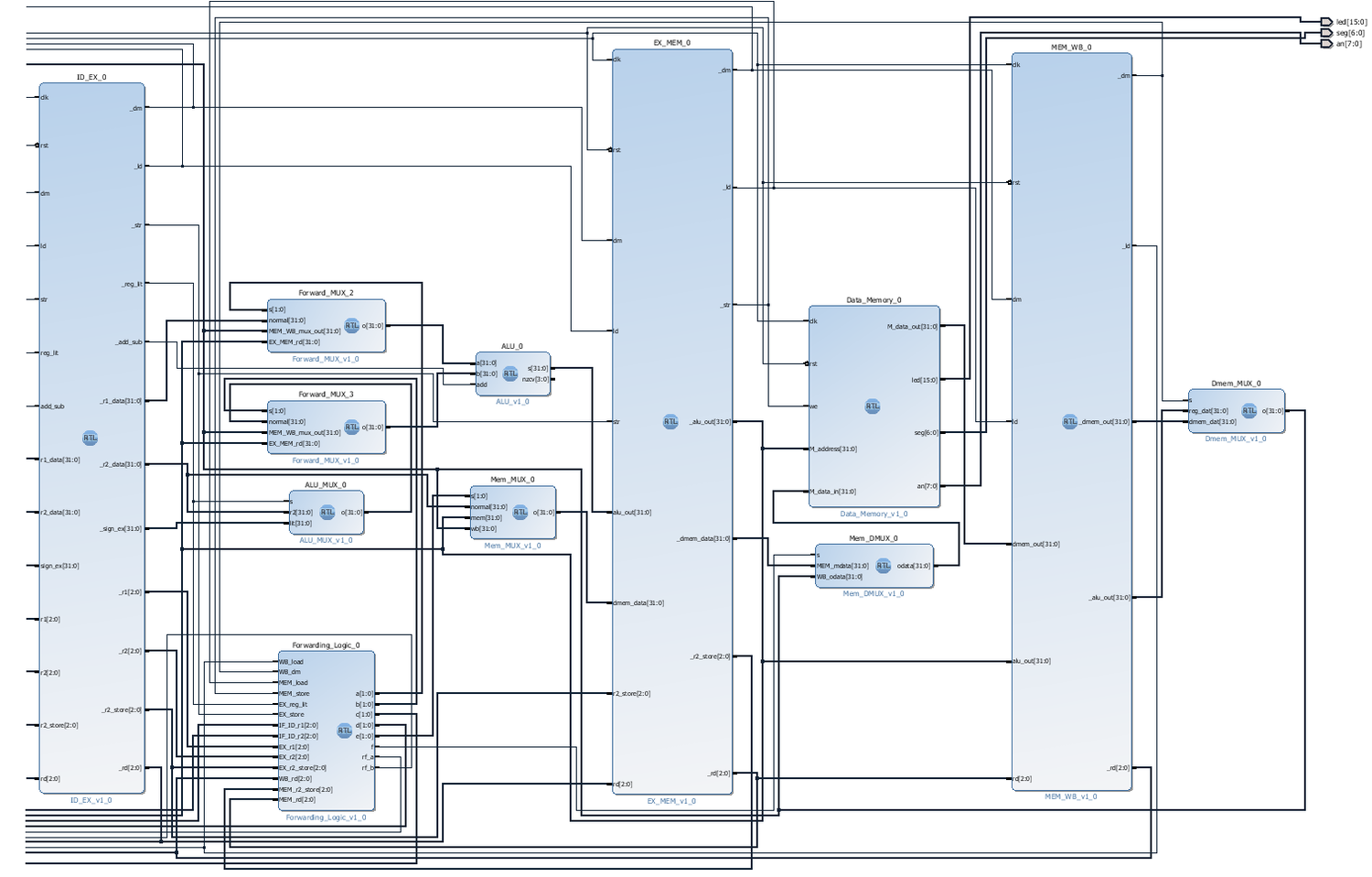
Pipelined Processor Final Report Simple Pipelined Processor RepositorySimple Pipelined Processor Block Diagram
Simple Pipelined Processor Programs
Five different programs were written to test the functionality of the processor. The programs are written in binary. The equivalent assembly language command is written in the comments next to each binary command. The commented section at the top of each file describes the operation of the program.
Simple Pipelined Processor ProgramsSimple Pipelined Processor Source
Finally, Below are the Verilog source files for the processor. Many of the files are very simple. Some of the files such as the register file and data memory are more complicated. Each of the Verilog files corresponds to a block in the block diagram above.
Simple Pipelined Processor Source