Viterbi Decoder Overview
I took a class on High Level Synthesis (HLS) techniques for logic design. I wanted to test and see how efficient any given HLS language was at producing logic when it was compared to an equivalent design written in VHDL or Verilog. I decided to write a Viterbi decoder using Xilinx Vivado HLS (C++) and run the synthesized output through Synopsys Design Compiler. I then used the Synopsys software to compile a Viterbi decoder written in VHDL from our textbook and compared the results. The results can be seen below, but the summary is the HLS design was about twice the area, consumed more power and was slower. Even though the performance of the HLS design was poorer in every way when compared to the VHDL design, it was easy to make and took a single day to design. The designs were compiled using a TMCS 90nm library. My conclusion is that HLS is not as efficient as Verilog or VHDL but can be practical if development time is critical.
Viterbi Decoder RepositoryViterbi Decoder Source Files
The HLS source was written with the same flow as the VHDL source code. The hope was to mimic the VHDL files and obtain the most efficient design possible.
Viterbi HLS Source Viterbi VHDL SourceArea and Power Report Summaries for the VHDL Decoder
Power Summary:
        Internal         Switching           Leakage            Total
        Power Group      Power            Power               Power              Power   (   %    )  Attrs
        --------------------------------------------------------------------------------------------------
        io_pad             0.0000            0.0000            0.0000            0.0000  (   0.00%)
        memory             0.0000            0.0000            0.0000            0.0000  (   0.00%)
        black_box          0.0000            0.0000            0.0000            0.0000  (   0.00%)
        clock_network      0.0000            0.0000            0.0000            0.0000  (   0.00%)
        register           0.0000            0.0000            0.0000            0.0000  (   0.00%)
        sequential         8.2150            1.0821        1.0759e+07           20.0558  (  10.34%)
        combinational    114.3817           50.1554        9.2800e+06          173.8171  (  89.66%)
        --------------------------------------------------------------------------------------------------
        Total            122.5968 uW        51.2375 uW     2.0039e+07 pW       193.8730 uW
Area Summary:
        Number of ports:                          141
        Number of nets:                           415
        Number of cells:                          289
        Number of combinational cells:            204
        Number of sequential cells:                85
        Number of macros/black boxes:               0
        Number of buf/inv:                         24
        Number of references:                      23

        Combinational area:               1939.968021
        Buf/Inv area:                      133.632003
        Noncombinational area:            2115.071974
        Macro/Black Box area:                0.000000
        Net Interconnect area:             219.201449

        Total cell area:                  4055.039995
        Total area:                       4274.241444
Area and Power Report Summaries for the HLS Decoder
Power Summary:
        Internal         Switching           Leakage            Total
        Power Group      Power            Power               Power              Power   (   %    )  Attrs
        --------------------------------------------------------------------------------------------------
        io_pad             0.0000            0.0000            0.0000            0.0000  (   0.00%)
        memory             0.0000            0.0000            0.0000            0.0000  (   0.00%)
        black_box          0.0000            0.0000            0.0000            0.0000  (   0.00%)
        clock_network      0.0000            0.0000            0.0000            0.0000  (   0.00%)
        register         177.2229           10.4321        2.9253e+07          216.9081  (  74.95%)
        sequential         0.0000            0.0000            0.0000            0.0000  (   0.00%)
        combinational     43.4242           13.8723        1.5181e+07           72.4781  (  25.05%)
        --------------------------------------------------------------------------------------------------
        Total            220.6472 uW        24.3044 uW     4.4435e+07 pW       289.3861 uW
Area Summary:
        Number of ports:                           10
        Number of nets:                            55
        Number of cells:                           45
        Number of combinational cells:             27
        Number of sequential cells:                17
        Number of macros/black boxes:               0
        Number of buf/inv:                          3
        Number of references:                       7

        Combinational area:               3526.963184
        Buf/Inv area:                      270.950407
        Noncombinational area:            5358.182343
        Macro/Black Box area:                0.000000
        Net Interconnect area:             474.999134

        Total cell area:                  8885.145527
        Total area:                       9360.144661
HLS Viterbi Decoder Waveform Simulation
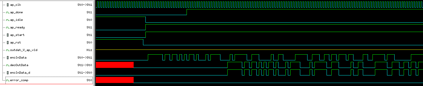
The following waveform shows the simulation of the HLS Viterbi decoder. decOutData Is the output of the decoder while encInData_d is the delayed input data. The delayed input signal timing matches that of the output and is used to look for decoding errors. error_comp is the comparison signal between the output and delayed input. It is low when the two signals match, and high when they are different. As can be seen, the decoder is producing the proper output for the duration of the simulation.
Viterbi Decoder FPGA Implementation
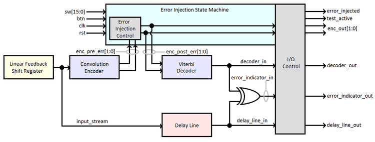
The group I was working with decided to implement the HLS Viterbi decoder in an FPGA and observe its functionality on an oscilloscope. The decoder was implemented on a Digilent Basys 3 FPGA development board. The Xilinx FPGA part number is XC7A35TCPG236-1. Below is the slide presentation which explains the test setup for the decoder and the observed results:
HLS Viterbi Decoder Implementation PresentationBelow are the source files for the project:
HLS Viterbi Decoder FPGA Source