Digital Down-Converter Overview
The DDC was to be designed with the following parameters:
1. The decimator input sample rate is 30.72MHz
2. The input signal is complex
3. The FPGA clock frequency is 245.76MHz
4. The peak filter sidelobe is to be -60dB with respect to the passband
Matlab Design Files
MATLAB files were given as a starting point for the design and were modified for this project's specifications.
Matlab FilesMatlab Design Plots
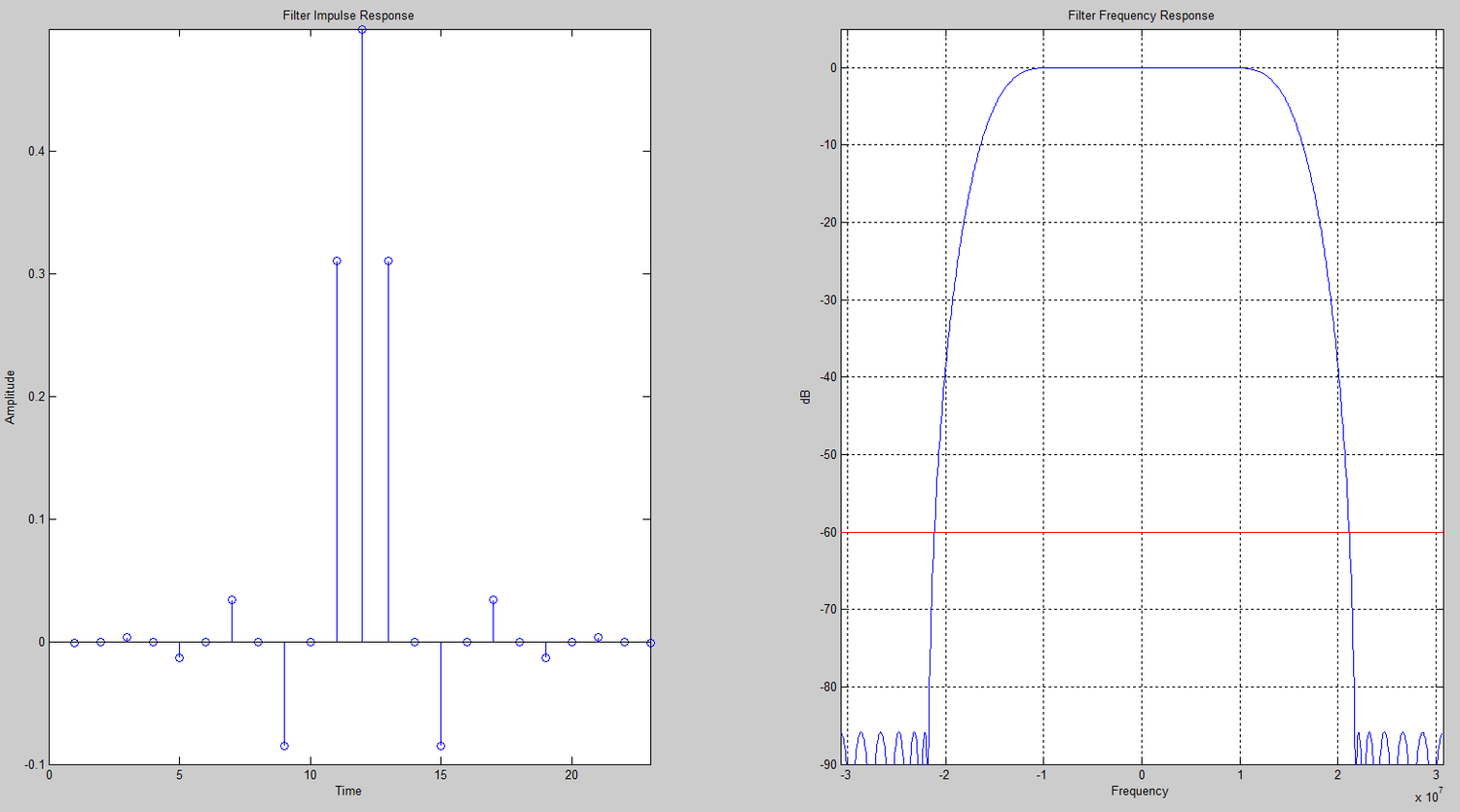
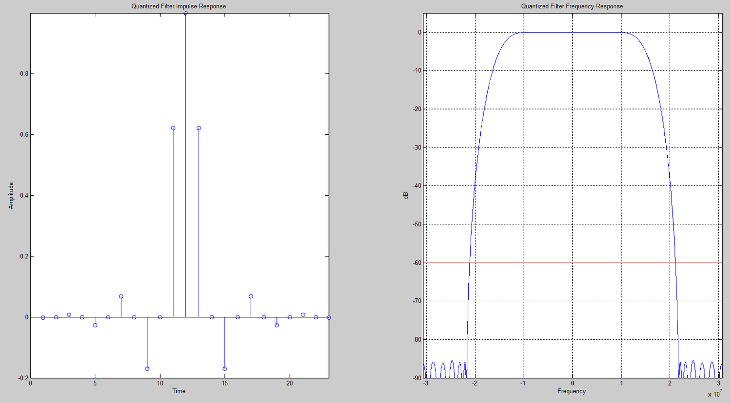
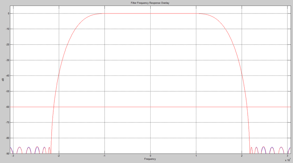
FPGA Implementation
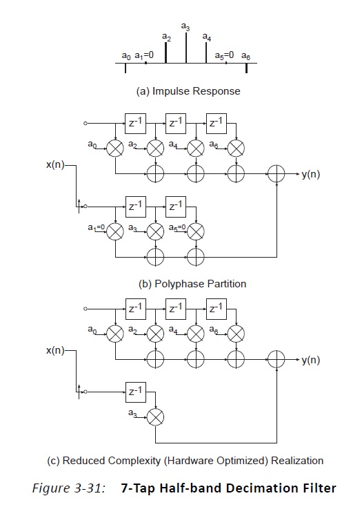
Vivado HLS Design Files
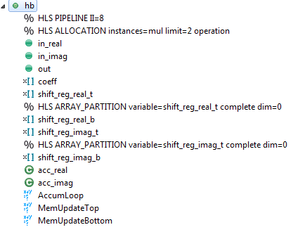
Next, the DDC was designed in HLS. The following is the HLS source code:
Vivado Design FilesVivado Design Results
The following is the calculated RMS error from the HLS test bench:
number of input test vectors = 50000
number of output test vectors = 25000
Real rms error = 5.83117e-005
% Real rms error = 0.00583117%
Imaginary rms error = 5.84182e-005
% Imaginary rms error = 0.00584182%
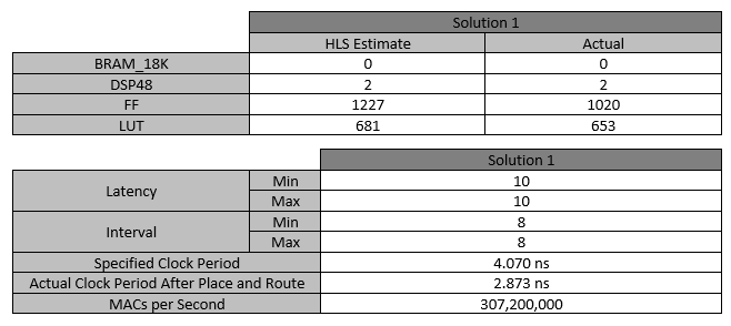
Next are the resource utilization and timing results for the solution:
Matlab Error Calculations
The MATLAB RMS error calculations are below and match the HLS calculations:
Number of output samples = 25000
RMS error, real = 0.000058
%RMS error, real = 0.005831%
RMS error, imaginary = 0.000058
%RMS error, imaginary = 0.005842%