Overview
I recreated the vector generator hardware for Asteroids in VHDL and simulated it using Modelsim. This simulation is a recreation of the hardware as it is on the PCB and is not designed for an FPGA. FPGAs do not support bidirectional signals (except at the I/O pins) and tri-state drivers. First, I built models of each of the individual integrated circuits. There are a total of 20 different ICs used in the vector generator. Second, I built the nine segments of the vector generator showed on the schematic. Third, I connected the nine sub-assemblies together to create the complete vector generator. Test benches for each of the IC models and assemblies were also created for a total of 60 VHDL files. The complete project can be found in the zipped file below. There is a macro file called wave.do that can be loaded to show some of the major signals during a simulation.
Asteroids HDL RepositoryBelow are various portions of the vector generator that I thought were interesting. I summarize the various opcodes and their formats and then explain various technical details of the vector generator. Some of the information below is described in the schematic but I thought is was interesting and restated it here. There is a lot of resources already on the internet about Atari vector generators and one of those resources can be found at:
http://www.jmargolin.com/vgens/vgens.htmInstruction Format
Below is a summary of the instruction format for the vector generator. It is also in the comments of the vector generator ROM. A lot of this information came from:
http://computerarcheology.com/Arcade/Asteroids/DVG.html
        ;------------------------------------------[ VEC Opcode ]------------------------------------------

        ;Draw a line from the current (x,y) coordinate.

        ;Example:
                      ;  SSSS -mYY YYYY YYYY | BBBB -mXX XXXX XXXX
        ;87FE 73FE    ;  1000 0111 1111 1110 | 0111 0011 1111 1110
                      ; - SSSS is the local scale 0 .. 9 added to the global scale
                      ; - BBBB is the brightness: 0 .. 15
                      ; - m is 1 for negative or 0 for positive for the X and Y deltas
                      ; - (x,y) is the coordinate delta for the vector

        ;VEC  scale=08(/2)   x=1022    y=-1022 b=07

        ;------------------------------------------[ CUR Opcode ]------------------------------------------

        ;Set the current (x,y) and global scale-factor.

        ;Example:
                      ; 1010 00yy yyyy yyyy | SSSS 00xx xxxx xxxx
        ;A37F 03FF    ; 1010 0011 0111 1111 | 0000 0011 1111 1111
                      ; - SSSS is the global scale 0 .. 15
                      ; - (x,y) is the new (x,y) coordinate. This is NOT adjusted by SSSS.

        ;CUR  scale=00(/512)  y=895  x=1023

        ;------------------------------------------[ HALT Opcode ]-----------------------------------------

        ;End the current drawing list.

        ;B000         ; 1011 0000 0000 0000

        ;HALT

        ;------------------------------------------[ JSR Opcode ]------------------------------------------

        ;Jump to a vector subroutine. Note that there is room in the internal "stack" for only FOUR levels
        ;of nested subroutine calls. Be careful.

        ;Example:
        ;        1100 aaaa_aaaa_aaaa
        ;             |||| |||| ||||
        ;          010aaaa_aaaa_aaaa0

        ;Address Conversion:
        ;$4000 + aaaa_aaaa_aaaa * 2

        ;------------------------------------------[ RTS Opcode ]------------------------------------------

        ;Return from current vector subroutine.

        ;D000         ; 1101 0000 0000 0000

        ;RTS

        ;------------------------------------------[ JMP Opcode ]------------------------------------------

        ;Jump to a new location in the vector program.

        ;Example:
        ;        1110 aaaa_aaaa_aaaa
        ;             |||| |||| ||||
        ;          010aaaa_aaaa_aaaa0

        ;Address Conversion:
        ;$4000 + aaaa_aaaa_aaaa * 2

        ;------------------------------------------[ SVEC Opcode ]-----------------------------------------

        ;Use a "short" notation to draw a vector. This does not mean the vector itself is necessarily
        ;short. It means that the notation is shorter (fewer bits of resolution).  In the hardware, the
        ;signal to indicate the SVEC command is being processed is ALPHANUM.  This indicates that the SVEC
        ;command is particularly useful for drawing numbers and letters on the display.

        ;Example:
                 ; 1111 smYY BBBB SmXX
        ;FF70    ; 1111 1111 0111 0000
                 ; - Ss This is added to the global scale
                 ; - BBBB is the brightness: 0 .. 15
                 ; - m is 1 for negative and 0 for positive for the X and Y
                 ; - (x,y) is the coordinate change for the vector

        ;SVEC scale=01(/256) x=0     y=-3    b=7
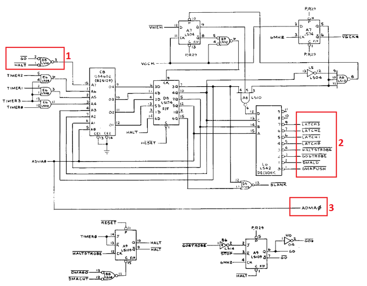
State Machine
The state machine is the brain of the vector generator and provides all the control signals. The ROM provides the next state logic. A breakdown of the contents of the ROM and how it is used follows.
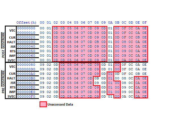
When the state machine ROM is loading a command, it is using the second half of the ROM. The rows
in the ROM represent the opcode being processed. The VEC opcode has 2 rows because it actually
has 10 different opcodes. It is important to note that the four TIMER signals are actually the
opcode bits. In the picture above and to the right, the three AND gates below the box with the "1"
next to it show that if the MSB of the opcode is clear, bits 6,5 and 4 of the address will all be zero.
This means all the VEC opcodes access the first and ninth row in the hex values above. If the final
VEC opcode (0x9) is being executed, the second and tenth row will be accessed. Notice that the ROM
is divided into 2 halves. The box labeled "1" in the schematic above show that the MSB of the address
will be cleared when neither halt_n nor go_n are active. This is the case when the opcode is being
fetched from memory. The signal gostrobe_n causes the fetched command to execute. At this point, the
MSB in the ROM address is set and effectively disables any further command signals from being issued
(the signals inside the box labeled "2").
The command signals are active when bit 3 is set on the ROM data line. This means that when the output
data from the ROM is 0x8, the dmapush_n is active, 0x9 maps to dmald_n all the way up to 0xF which maps
to latch3_n. The data nibble at each address in the state machine ROM represents the next state to be
executed. This means that if the current data out is a 0x9, then the next column to be accessed in the
hex values above will be column 0x9. Notice the upper half of the ROM in column 0x1 all have 0x1 in it.
This is the waiting area that the state machine sits in while a command is being executed. When the go_n
signal goes high at the completion of the command, the second half of the ROM becomes active and the next
instruction is fetched.
The adma0 bit for the vector ROM address is generated by the state machine itself and is based on the LSB
of the data. This means that the vector ROM is not necessarily accessed in ascending order. Also,
gostrobe_n is activated when the data output of the state machine ROM is 0xA. This is the point when the
instruction fetch is complete and the execution begins. This is also when the state machine ROM switches
from the lower portion of the ROM to the upper portion (with respect to the hex data graphic above).
Vector Generator Memory Data Latches
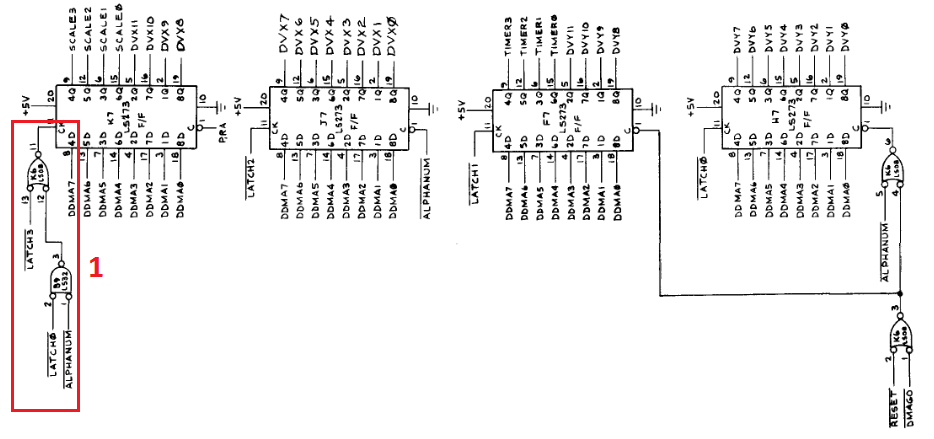
The vector memory data latches are straight forward except for the piece of logic in the box labelled "1". The alphanum_n signal is active when the SVEC command is being fetched and executed. Since the SVEC command is only two bytes, the logic above overrides the latch3_n signal and loads portions of the SVEC data during the latch0_n phase of the fetch.
X and Y Position Counters
The rate multiplier chip (sn7497) is an interesting chip. it only allows a certain number of clock cycles to appear on the output for every 64 clock cycles on the input. The number of clock cycles allowed is determined by the value being applied to the "b" input of the chip. The output clock cycles are not necessarily evenly spaced. The sn7497 can be cascaded with other rate multipliers to make the scaling go beyond 6 bits. Below are some simulation results of the chip to show how it works. In the first picture, the input is set to 19. This means there are 19 output clocks for every 64 input clocks. The second and third picture show the outputs when the input values are set to 31 and 5 respectively.


The description of the X and Y counter is quite thorough in the schematic. Below are some waveforms from the simulation that show the operation of the counters at their maximum and minimum extent and their relation to the beam valid signal. When an X or Y counter hits its maximum value, it it locked at the value and the beam valid signal goes low. This keeps the bean from wrapping around to the other side of the screen and turns it off. The red squares in the pictures below highlight this behavior in the simulation. Even though the output of the counter is being held at its minimum/maximum value on the output, the counter is actually still counting and could theoretically roll over and become valid again. This would take a long time and should never happen in practice.


Vector Timer
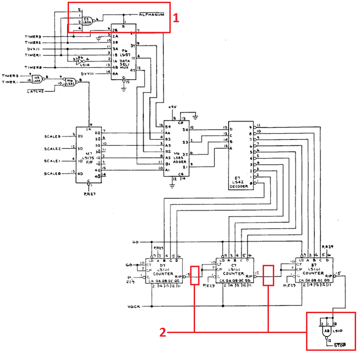
The vector timer controls how long a vector is drawn for. There are a couple of interesting this to highlight in
this circuit. First, the alphanum_n signal is generated here as shown in the red box labelled "1". The alphanum_n
signal is active when all four of the opcode bits are set (0xF). This is the SVEC opcode. Among other things, it
switches the scaling between SVEC and VEC scaling. Details of scaling are described below and can also be found in
the asteroids vector ROM assembly file.
During simulation, the stop_n output and ripple carry outputs highlighted by the boxes labelled "2" have glitches
in them. After reviewing the HDL design, I realized that this was the correct behavior of the LS161 counters. I
also noticed in the Star Wars PCB schematic, the ripple carry outputs are ANDed with all previous ripple carry
outputs. This is most likely to prevent the glitching seen on the Asteroids board. Below is a simulation example
of the glitching seen in the stop_n signal.

Below are the details of how the Asteroids game scaling system works.
        ;Scaling is a major factor and comes from multiple sources.  There is a global scaling modifier
        ;that is set with the CUR opcode.  The VEC opcode sets a local scaling factor for the current
        ;vector being drawn.  The SVEC opcode also has a scaling factor that is different than the VEC
        ;scaling factor.  The total scaling is a combination of the VEC/SVEC scaling factor and the
        ;global scaling modifier.  The scaling factor and modifier can be associated with both a number
        ;and multiplier.  Both will be discussed here.

        ;It should be noted that a total scaling factor of 9 means that the vector's XY components have
        ;a range of +/- 1023 units. The display is 1024 units wide and tall, therefore a total scaling
        ;factor of 9 is equal to screen width(or height)/1-1.  A total scaling factor of 0 is equal to
        ;screen width/512-1 which means the vector has a range of +/- 1 in the X or Y directions.

        ;-----------------------
        ;Global Scaling Modifier
        ;-----------------------
        ;The 32-bit CUR command has the following format:
        ;1010 00yy yyyy yyyy | SSSS 00xx xxxx xxxx
        ;A detailed explanation of the command can be found in the CUR opcode section.  For this section,
        ;the SSSS is of interest because it sets the global scaling modifier.  The global scaling number
        ;is the signed 4-bit SSSS value.  The global scaling number and its associated scaling multiplier
        ;are listed in the following table:

        ;     Global Scaling Modifier
        ;----------------------------------
        ;  Bits  |  Number  |  Multiplier
        ;  1000  |    -8    |    1/256
        ;  1001  |    -7    |    1/128
        ;  1010  |    -6    |    1/64
        ;  1011  |    -5    |    1/32
        ;  1100  |    -4    |    1/16
        ;  1101  |    -3    |    1/8
        ;  1110  |    -2    |    1/4
        ;  1111  |    -1    |    1/2
        ;  0000  |     0    |    1
        ;  0001  |     1    |    2
        ;  0010  |     2    |    4
        ;  0011  |     3    |    8
        ;  0100  |     4    |    16
        ;  0101  |     5    |    32
        ;  0110  |     6    |    64
        ;  0111  |     7    |    128

        ;------------------
        ;VEC Scaling Factor
        ;------------------
        ;The VEC opcode is actually the scaling factor.  The VEC command has the following format:
        ;SSSS -mYY YYYY YYYY | BBBB -mXX XXXX XXXX
        ;The scaling number for this reason is limited to 0-9.  The bits of the scaling factor can
        ;be thought of as an unsigned number.  The VEC scaling number and its associated scaling
        ;multiplier are listed in the following table:

        ;     VEC Scaling Factor
        ;----------------------------------
        ;  Bits  |  Number  |  Multiplier
        ;  0000  |    0     |    1/512
        ;  0001  |    1     |    1/256
        ;  0010  |    2     |    1/128
        ;  0011  |    3     |    1/64
        ;  0100  |    4     |    1/32
        ;  0101  |    5     |    1/16
        ;  0110  |    6     |    1/8
        ;  0111  |    7     |    1/4
        ;  1001  |    8     |    1/2
        ;  1001  |    9     |    1

        ;-------------------
        ;SVEC Scaling Factor
        ;-------------------
        ;The SVEC command has the following format:
        ;1111 smYY BBBB SmXX
        ;The scaling factor is Ss.  The 2 Scaling bits get remapped in the hardware to match bits in the
        ;VEC command.  The 2-bit SVEC scaling number, its remapped bits and its associated scaling
        ;multiplier are listed in the following table:

        ;               SVEC Scaling Factor
        ;--------------------------------------------------
        ;  Bits  |  Remapped Bits  |  Number  |  Multiplier
        ;   00   |      0010       |    2     |    1/128
        ;   01   |      0011       |    3     |    1/64
        ;   10   |      0100       |    4     |    1/32
        ;   11   |      0101       |    5     |    1/16

        ;-------------------
        ;Total Scaling Value
        ;-------------------
        ;The scaling factor and scaling modifier numbers can be added together to form a total scaling
        ;number:

        ;Total Scaling Number = VEC(or SVEC) Scaling Number + Global Scaling Number

        ;The associated total scaling multiplier can be found in the VEC table in the same row as the
        ;resulting number.  Also, the total scaling factor can be calculated as:

        ;Total Scaling Multiplier = VEC(or SVEC) Scaling Multiplier * Global Scaling Multiplier

        ;As with the VEC command, the SVEC scaling number and its associated multiplier are in the same
        ;table row.  It should be noted that a scaling number outside the range of 0-9 is not valid.  It
        ;will load the vector timer with all 1s and cause it to expire on the next clock cycle.  The
        ;easiest way to calculate the scaling number is to add the 4-bit values together and ignore the
        ;carry.  In the case of SVEC, use the remapped bits.  Then, look up the 4-bit value in the VEC
        ;scaling factor table.  Here are some examples:

        ;                       Bits Number Multiplier
        ;Global scaling value:  0011    3      8
        ;VEC scaling value:    +0101   +5    *1/16
        ;                      -----  -----  -----
        ;Total scaling value:   1000    8     1/2

        ;                       Bits Number Multiplier
        ;Global scaling value:  1101   -3     1/8
        ;SVEC scaling value:   +0100   +4    *1/32
        ;                      -----  -----  -----
        ;Total scaling value:   0001    1    1/256

        ;                       Bits Number Multiplier
        ;Global scaling value:  0101    5     32
        ;SVEC scaling value:   +0101   +5    *1/16
        ;                      -----  -----  -----
        ;Total scaling value:   1010   10      2     INVALID!

        ;                       Bits Number Multiplier
        ;Global scaling value:  1000   -8    1/256
        ;VEC scaling value:    +0100   +4    *1/32
        ;                      -----  -----  -----
        ;Total scaling value:   1100   -4    1/8192  INVALID!

        ;As can be seen from the examples above, A total scaling number outside the range 0 to 9 is
        ;invalid and a total scaling factor outside the range 1 to 1/512 is invalid.  Also note that the
        ;numbers wrap around.  That means that 1100 = -4 can also be interpreted as 12.  Both are invalid.
        ;In terms of hardware, the invalid range occurs because the two values are added together and the
        ;result is passed into a BCD to decimal decoder.  If the 4-bit BCD value is greater than 9, the
        ;decoder simply turns on all its output bits, causing the timer to load with its maximum value.
Full Simulation
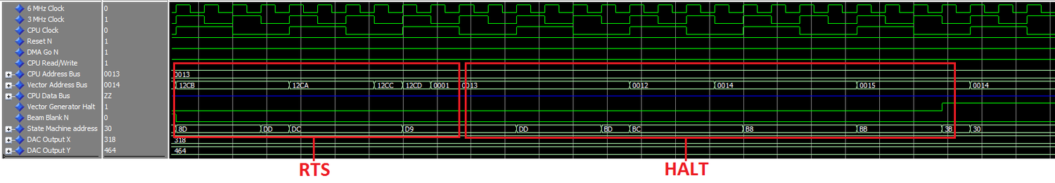
A simple simulation is provided in the top level testbench that exercises all seven opcodes. It draws the letter "A" and also the ship's thrust graphic to the output. It also set the beam position and performs a jump operation. Below is a picture from the simulator of the entire sequence.
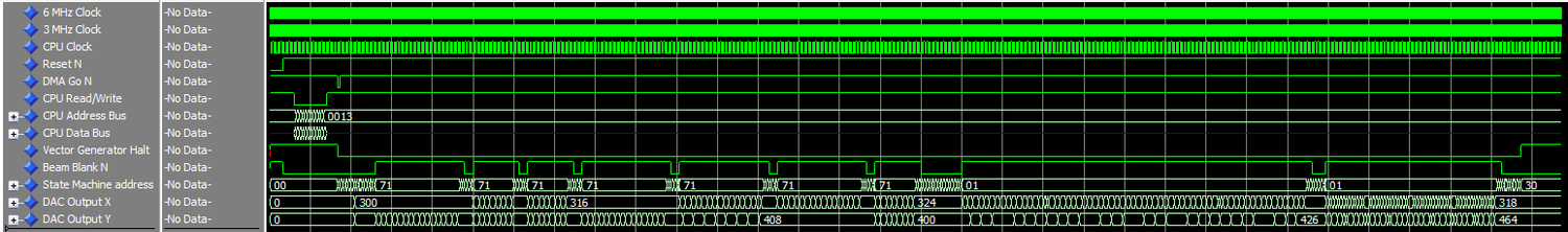
Zooming in on the first section shows the system coming out of reset and the CPU loading all the instructions to be executed into the vector RAM. Once the data is loaded, the CPU releases control of the address and data lines and strobes the dma go signal to start the vector state machine.
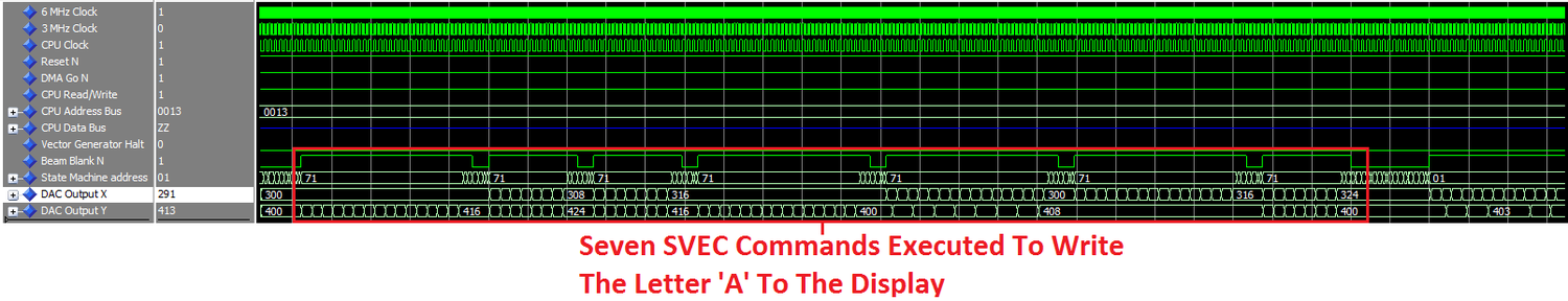
When the vector generator starts executing, it first sets the beam to position 300,400 on the display with the CUR command. It then jumps to the subroutine in the vector generator ROM for writing an 'A' to the display.
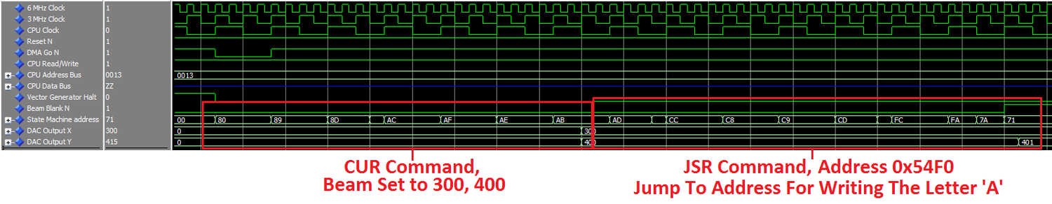
The letter 'A' is then drawn on the display using seven separate SVEC commands.
Next, The vector generator returns from the character drawing subroutine. It then jumps to address 0x0010 to test the JMP instruction. Another JSR command is executed to draw a ship thrust graphic.
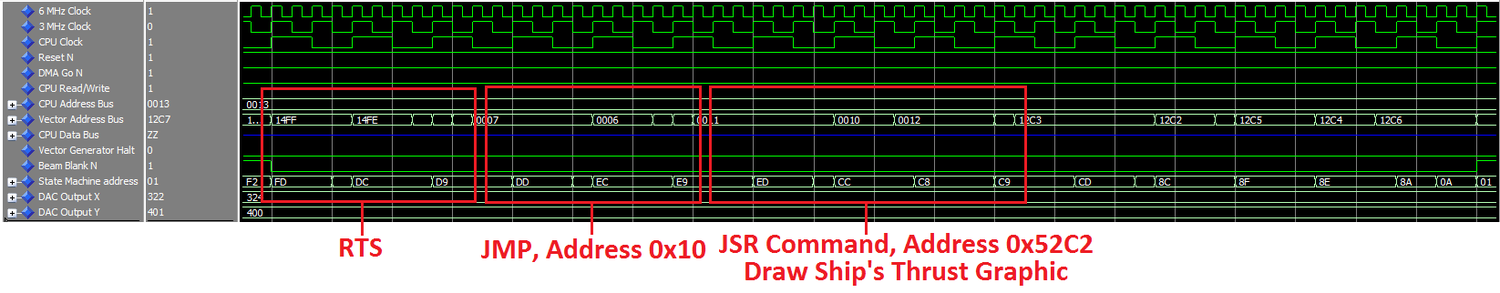
Two VEC commands are then executed to draw the ship's thrust graphic to the display.
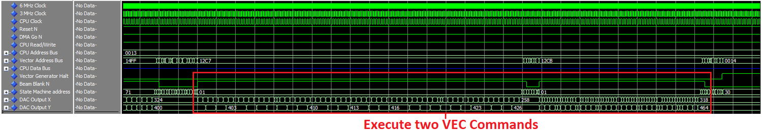
Finally, The vector generator returns from the ship thrust subroutine and executes the HALT instruction putting it into an idle state.